


A team of physicists has succeeded in highlighting the movement of a single atom in a silicon crystal, capable of jumping, under laser excitation, between several positions in a fluorescent defect.
Reading time: 3 minutes
|
Key facts:
|
Crystalline fluorescent defects in semiconductor materials are fascinating quantum systems because they behave like artificial atoms trapped in the crystal. Among the many possible defects in the crystal of silicon, the flagship material of microprocessors, there is a particularly interesting defect, well known since the 1970s and called the G centre. The study of this defect has seen a resurgence in recent years due to its spin properties combined with the emission of single photons at telecom wavelengths. Usually, defects have a static microscopic structure where atoms are only allowed to vibrate around well-defined equilibrium positions, without being able to make larger excursions. Surprisingly, this is not the case for centre G, which consists of 2 carbon impurities, linked by an interstitial silicon atom that can move between 6 crystal sites (see figure).
This effect had never before been observed on the scale of the individual defect, a feat recently achieved by an international collaboration involving researchers in France and Hungary (see below). By isolating a single G defect using advanced low-temperature microscopy techniques, the scientists detected a fine structure in its emission lines that is the signature of the movement of a single silicon atom within the massive crystal containing billions of billions of silicon atoms.
By analysing the emission properties of individual G centres, the researchers have also shown that their dynamics are very sensitive to perturbations in the crystalline environment. In particular, the samples commonly used in microelectronics and nanophotonics, consisting of a layer of silicon on a layer of SiO2 silica, have a stress that distorts the geometric structure of the defects. As a result, the mobile atom of the G centres, which is perfectly delocalised between the 6 sites in the undisturbed case, finds itself trapped in a given site. Laser excitation then causes it to jump randomly between the different positions, like a marble in a 6-slot casino roulette wheel.
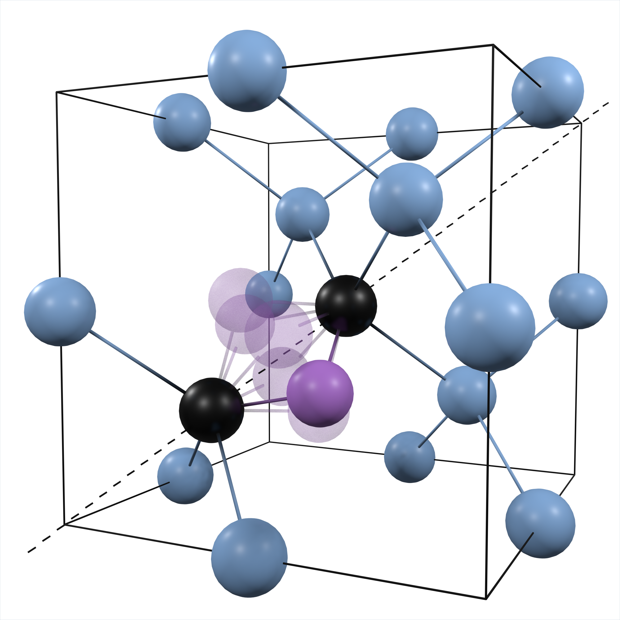
View of a G center whose central atom jumps from one site to another. The carbon atoms appear in black, the interstitial silicon atom in violet and the other silicon atoms in the crystal in blue.
Single-photon sources and spin-photon interfaces exploiting the properties of individual G centres are of interest in the context of the burgeoning development of quantum photonics integrated on silicon chips. So the next challenge for researchers will be to control the reconfiguration dynamics of individual G centres. Future avenues of exploration include engineering the deformation of the silicon crystal and developing resonant laser excitation protocols to force the mobile atom to remain in a given crystal site. This work is published in the journal Physical Review X.
Contact à ajouter
References:
A. Durand et al, Hopping of the Center-of-Mass of Single G Centers in Silicon-on-Insulator, Physical Review X 14, 041071 (2024) - Published December 27, 2024
Article originally published on the CNRS website on Monday, May 26, 2025.
Figure credit: Félix Cache, L2C, CNRS and Université de Montpellier.
Discover also


Share on social media or